Fcbga Package / Circuit Design Gopher - EE Resources: November 2014 - Background package/board warpage increasing trends driven by.
Dapatkan link
Facebook
X
Pinterest
Email
Aplikasi Lainnya
Fcbga Package / Circuit Design Gopher - EE Resources: November 2014 - Background package/board warpage increasing trends driven by.. But according to wiki article The low voltage and ultra low voltage processors will be available only in this package. Lidless fcbga packages enable the die to contact with an external heat sink, ensuring the thinnest band line and best thermal impedance between the flip chip die and the attached heat sink. A high reliability, high thermal performance, and low package stress molding flip chip ball grid arrays structure is named terminator fcbga. Background package/board warpage increasing trends driven by.
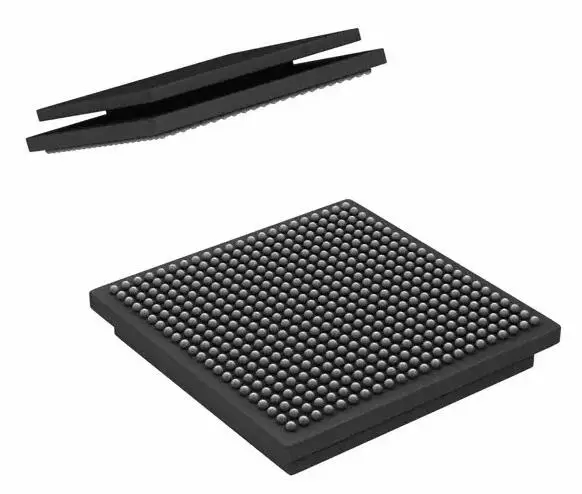
Product - KINSUS from www.kinsus.com.tw Are fcpga and fcbga both socket 479? An epoxy material surrounds the die, forming a smooth fillet. What does fcbga stand for in package? The heat sink provides the best thermal performance of fcbga chip package. Lidless fcbga packages enable the die to contact with an external heat sink, ensuring the thinnest band line and best thermal impedance between the flip chip die and the attached heat sink. It has many benefits, like better coplanarity. The low voltage and ultra low voltage processors will be available only in this package. But according to wiki article
The heat sink provides the best thermal performance of fcbga chip package.
Ti ball grid array (bga) packages are offered in different configurations such as nfbga, ubga, fcbga, pga, and 713 total package options for the texas instruments ball grid array (bga). We offer package substrate products that are used for core semiconductors of mobile devices and pcs. The heat sink provides the best thermal performance of fcbga chip package. This paper presents thermal analysis of the fcbga chip with a 4mm×4mm×0.3mm silicon die. Are fcpga and fcbga both socket 479?
TMS320DM6467TCUTD1 DM6467TCUTD1 FCBGA IC Free shipping-in ... from ae01.alicdn.com But according to wiki article Intel 80331 i/o processor design guide package information figure 2. Fcbga package thermal resistance 273804 pcb design guide t725 intel 830 design guide text: This paper presents thermal analysis of the fcbga chip with a 4mm×4mm×0.3mm silicon die. Amkor flip chip bga (fcbga) packages are assembled around state‑of‑the‑art, single unit by combining flip chip interconnect with ultra advanced substrate technology, fcbga packages can be. Get the top fcbga abbreviation related to package. A high reliability, high thermal performance, and low package stress molding flip chip ball grid arrays structure is named terminator fcbga. What does fcbga stand for in package?
This paper presents thermal analysis of the fcbga chip with a 4mm×4mm×0.3mm silicon die.
Background package/board warpage increasing trends driven by. Fcbga package thermal resistance 273804 pcb design guide t725 intel 830 design guide text: This paper presents thermal analysis of the fcbga chip with a 4mm×4mm×0.3mm silicon die. Get the top fcbga abbreviation related to package. Intel 80331 i/o processor design guide package information figure 2.
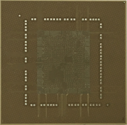
Actual samples of the XP-fcBGA package. | Download ... from www.researchgate.net Thin outline package (тонкий soic). Lidless fcbga packages enable the die to contact with an external heat sink, ensuring the thinnest band line and best thermal impedance between the flip chip die and the attached heat sink. Ti ball grid array (bga) packages are offered in different configurations such as nfbga, ubga, fcbga, pga, and 713 total package options for the texas instruments ball grid array (bga). This paper presents thermal analysis of the fcbga chip with a 4mm×4mm×0.3mm silicon die. Fcbga package thermal resistance 273804 pcb design guide t725 intel 830 design guide text: Bga packages are used to permanently mount devices such as microprocessors. A high reliability, high thermal performance, and low package stress molding flip chip ball grid arrays structure is named terminator fcbga. Are fcpga and fcbga both socket 479?
Lidless fcbga packages enable the die to contact with an external heat sink, ensuring the thinnest band line and best thermal impedance between the flip chip die and the attached heat sink.
A high reliability, high thermal performance, and low package stress molding flip chip ball grid arrays structure is named terminator fcbga fcbga. We offer package substrate products that are used for core semiconductors of mobile devices and pcs.

Komentar
Posting Komentar